
Germany Silicon Carbide (SiC) Wafer Market Size & Forecast 2025–2034
How EV Electrification, Renewable Energy Expansion, and Semiconductor Localization Are Powering Germany’s SiC Wafer Growth

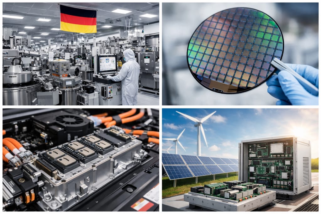
Introduction
The Germany Silicon Carbide (SiC) Wafer Market is entering a decisive growth phase as the country accelerates electrification, clean-energy deployment, and advanced semiconductor manufacturing. According to Renub Research, the market was valued at US$ 48.49 million in 2025 and is projected to grow at a compound annual growth rate (CAGR) of 12.41% between 2026 and 2034, reaching US$ 138.96 million by 2034.
This expansion reflects Germany’s leadership in automotive engineering, industrial automation, and renewable energy infrastructure. Silicon carbide wafers—known for superior thermal conductivity, high breakdown voltage, and exceptional energy efficiency—are becoming essential substrates for next-generation power electronics. From electric vehicles and fast-charging networks to wind turbines and smart grids, SiC wafers are enabling Germany’s transition toward a cleaner, more resilient, and technologically advanced economy.
Outlook of the Germany Silicon Carbide Wafer Market
Silicon carbide is a wide-bandgap semiconductor that significantly outperforms conventional silicon in high-power, high-temperature, and high-frequency environments. Its intrinsic material properties allow devices to operate at higher voltages and switching frequencies with lower power losses, making SiC indispensable for modern power electronics.
Germany’s industrial ecosystem strongly aligns with these advantages. The nation’s automotive sector increasingly relies on SiC-based inverters and onboard chargers to enhance EV range, reduce system weight, and improve overall efficiency. Simultaneously, the renewable energy sector uses SiC devices to increase the efficiency and durability of solar inverters, wind power converters, and grid-stabilization systems.
Germany also hosts a dense network of research institutions, applied laboratories, and semiconductor manufacturers focused on improving SiC wafer quality, reducing defect density, and scaling up production to larger diameters. As power electronics become the backbone of electrified mobility, renewable energy, and industrial automation, silicon carbide wafers are emerging as a strategic material for Germany’s long-term technological competitiveness.
Key Growth Drivers in the Germany Silicon Carbide Wafer Market
Rapid Electrification of Vehicle Powertrains
Germany’s position as one of the world’s largest automotive manufacturing hubs makes EV adoption a primary driver of SiC wafer demand. Silicon carbide devices enable higher efficiency in traction inverters and onboard chargers, directly improving vehicle range and charging speed while reducing cooling requirements.
In 2025, Germany recorded 434,627 battery electric vehicle (BEV) sales, reclaiming its status as Europe’s largest EV market. German OEMs and Tier-1 suppliers increasingly integrate SiC power modules into next-generation vehicle platforms, accelerating wafer demand across domestic supply chains.
Expansion of Renewable Energy and Grid Modernization
Germany’s ambitious energy transition targets further reinforce SiC adoption. The country achieved nearly 57% of gross power demand from renewables in the first three quarters of 2025 and aims to reach 80% by 2030. In 2024 alone, Germany added 20 GW of renewable capacity, driven largely by solar photovoltaics and onshore wind.
SiC wafers enable higher efficiency and power density in renewable energy converters, hydrogen electrolysis systems, and high-voltage direct current (HVDC) infrastructure. Their superior thermal stability improves system reliability under variable load conditions, making them ideal for decentralized grids and energy storage applications.
Advancement of Domestic Semiconductor Manufacturing
Germany’s semiconductor strategy emphasizes supply-chain resilience and technological sovereignty. In 2025, federal and state governments redirected billions of euros toward semiconductor R&D, pilot fabs, and advanced manufacturing infrastructure. These investments support local epitaxy, device fabrication, and wafer production capabilities, reducing dependence on overseas suppliers.
Collaborations between industry and research institutions focus on scaling SiC wafer diameters, improving yield, and lowering defect density—critical factors for mass adoption in automotive and industrial markets.
Challenges Facing the Germany SiC Wafer Market
High Production Costs and Yield Limitations
Despite its advantages, SiC wafer production remains capital-intensive. Crystal growth, slicing, polishing, and epitaxial processing are complex and energy-intensive, with defects such as micropipes and dislocations impacting yield. Transitioning to 150 mm and 200 mm wafer production requires significant investment in equipment and cleanroom upgrades, creating barriers for smaller manufacturers.
Supply-Chain Bottlenecks and Standardization Issues
The global SiC supply chain is still maturing. Limited suppliers of high-purity raw materials, seed crystals, and specialized crucibles expose manufacturers to price volatility and supply disruptions. Inconsistent quality standards across suppliers complicate device qualification and slow commercialization. Strengthening domestic precursor supply and harmonizing testing standards remain critical priorities.
Germany 6-Inch Silicon Carbide Wafer Market
The 6-inch (150 mm) SiC wafer segment plays a transitional role between legacy 100 mm wafers and emerging 200 mm technologies. These wafers offer improved economies of scale while maintaining compatibility with established fabrication processes. In Germany, 6-inch wafers are widely used for automotive, industrial, and renewable energy devices, enabling manufacturers to refine yield strategies before full-scale adoption of larger diameters.
Germany Semi-Insulating Silicon Carbide Wafer Market
Semi-insulating (SI) SiC wafers are critical for RF, microwave, and high-frequency applications. In Germany, demand arises from radar systems, telecommunications infrastructure, aerospace electronics, and industrial plasma systems. These wafers command premium pricing due to stringent requirements for resistivity uniformity and defect control, serving niche but high-value markets.
Germany Power Electronics Silicon Carbide Wafer Market
Power electronics represent the largest application segment for SiC wafers in Germany. EV traction inverters, renewable energy converters, industrial motor drives, and UPS systems rely on SiC substrates to achieve higher efficiency and compact designs. As electrification spreads across industries, demand for high-quality SiC wafers continues to rise.
Germany Telecommunications Silicon Carbide Wafer Market
In telecommunications, SiC wafers support high-power RF devices used in base stations, remote radio heads, and millimeter-wave systems. While GaN dominates RF amplification, SiC substrates remain essential for thermal management and high-power operation in demanding outdoor environments.
Germany Aerospace and Defense Silicon Carbide Wafer Industry
Aerospace and defense applications require components that operate reliably under extreme conditions. SiC wafers enable high-temperature, radiation-resistant power electronics for satellites, radar systems, and electronic warfare platforms. Germany’s defense contractors value locally sourced, aerospace-grade SiC wafers that meet rigorous qualification standards.
Regional Market Dynamics
Frankfurt serves as a logistics and distribution hub, supporting wafer testing, storage, and international trade.
Munich drives demand through automotive R&D, power electronics innovation, and strong academic-industry collaboration.
Berlin acts as an innovation catalyst, with start-ups developing niche SiC-based solutions for renewable energy and mobility.
Market Segmentation Overview
By Wafer Diameter: ≤4 inch, 6 inch, 8 inch, ≥12 inch
By Conductivity Type: N-Type Conductive, Semi-Insulating
By Application: Power Electronics, RF Devices, Optoelectronics, Others
By End-Use: Automotive & EVs, Renewable Energy, Telecom, Industrial Drives, Aerospace & Defense
By Crystal Growth Technology: PVT, CVD, Modified Lely, Others
By Cities: Frankfurt, Munich, Hamburg, Berlin, Stuttgart, Düsseldorf, and others
Competitive Landscape
Major companies operating in the Germany SiC wafer ecosystem include:
Wolfspeed Inc.
Coherent Corp.
Xiamen Powerway Advanced Material Co., Ltd.
STMicroelectronics N.V.
Resonac Holdings Corporation
SK Siltron Co., Ltd.
SiCrystal GmbH
Each company is analyzed across five viewpoints: overview, key personnel, recent developments, SWOT analysis, and revenue performance.
Final Thoughts
The Germany Silicon Carbide Wafer Market is poised for sustained expansion through 2034, driven by electrified mobility, renewable energy growth, and semiconductor localization strategies. While high production costs and supply-chain challenges persist, continued investment in R&D, manufacturing scale-up, and quality standardization will strengthen Germany’s position in the global SiC ecosystem.
As EV adoption accelerates and energy systems demand higher efficiency and resilience, silicon carbide wafers will remain a foundational technology supporting Germany’s clean-energy ambitions and industrial leadership.
About the Creator
Keep reading
More stories from shibansh kumar and writers in Trader and other communities.
Europe Books Market Size and Forecast 2026–2034
Europe Books Market Overview The Europe books market is projected to expand steadily over the coming decade, increasing from US$ 44.68 billion in 2025 to US$ 62.29 billion by 2034. According to Renub Research, this growth reflects a compound annual growth rate (CAGR) of 3.76% during 2026–2034, driven by strong educational demand, rising audiobook consumption, expanding online retail channels, and continuous content innovation by publishers across major European economies.
By shibansh kumarabout 13 hours ago in Trader
smci stock: Is This the Breakout Investors Have Been Waiting For?
Many investors are eyeing smci stock as hidden signals point to a possible breakout. Understanding these signals can help investors make smart decisions and prepare for potential gains. In this article, we explore why smci stock is gaining attention and what factors could drive its next move.
By John.doe7983 days ago in Trader
Ice Makers on Demand: Market Trends Powering a Cool Revolution
Ice Maker Market Overview The global Ice Maker Market continues to expand steadily as demand rises from commercial, industrial, and residential sectors driven by growth in the foodservice, hospitality, healthcare, and retail industries. Ice makers — machines that automatically produce ice cubes, flakes, nugget ice, and specialty formats — are essential for beverage cooling, food preservation, medical applications, and household convenience.
By James Smith5 days ago in Trader


Comments
There are no comments for this story
Be the first to respond and start the conversation.